Technology Ultrashort pulse laser
The continuous increase in the integration density of electronic products, rising requirements for stability and structure resolution, and increased functional integration in components through the provision of functional structures and geometries are leading to a growing demand for suitable manufacturing techniques that enable production to produce components with structures in the micrometre range with accuracies in the nanometre range.
Laser technology enables high-performance manufacturing solutions and has proven this for many years in numerous applications. With the development of high-power ultrashort pulse lasers in the early 2000s, a class of laser beam sources conquered industrial practice. Ultrashort pulse lasers with pulse durations in the femto and picosecond range (10 – 15 p– 10 – 12 s) open up completely new machining processes and enable the highest machining precision down to the nanometer range.
Materials of any kind, such as metals, ceramics, semiconductors, polymers and even biomaterials can be processed with the highest precision and without additional tools. With the ultrashort pulse laser, a tool-free “photonic milling machine” is available which, if used correctly, provides a high degree of precision and flexibility in production.

The outstanding feature of ultra-short pulse processing compared to longer-pulsed laser systems such as nanosecond lasers are the strong localization of the energy input as well as the targeted use of nonlinear absorption mechanisms in the material to be processed. A large number of investigations have shown that particularly high ablation qualities can be achieved, especially with pulse durations of less than 15 ps, since an interaction between the laser beam and ablation products of the same laser pulse can be largely avoided, especially with metals, and the material primarily evaporates instead of as an explosive melt To leave the processing location.
The application of ultra-short pulses leads to a Avoidance of enamel deposits, whereby high processing quality can be achieved in applications for ablating, drilling holes or cutting metal foils. The generated lateral structures are often in the range from 10 µm to a few 100 µm, but due to the low heat losses in the surrounding material, much higher lateral resolutions down to the sub-µm range can be achieved with USP processing.
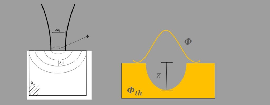
The photons hitting the workpiece interact primarily with the electrons of the solid, so that the energy of the laser is initially deposited in the electron system. The energy transfer of the electrons to the lattice structure of a solid takes place with a time delay with material-specific time constants, which for metals are typically in the range of a few picoseconds. Only (> 100 ps) phase transitions up to evaporation and ablation of the material occur. At this point in time, however, the laser pulse has already ended, so that, in contrast to the previous nanosecond ablation with laser radiation, no interaction can take place between the incident laser beam and the material vapor generated. By coupling the energy of the laser pulse in an extremely short time and the immediately following ablation process the energy remains strongly localized at the point of impact of the laser beam and hardly dissipates into surrounding areas. This results in an extremely high structural resolution without heating up the surrounding areas.
In addition to these “thermal” arguments, the extremely high intensities also generate> 10^12 W / cm 2 when processing with ultrashort pulse lasers, there are clear advantages in processing. Due to nonlinear absorption phenomena semiconductors and insulators such as silicon, glass, sapphire and ceramics can also be processed with high efficiency.
The ultra-short pulse laser processing enables a extremely large application potential which has new manufacturing technology solutions for many industrial issues and enables product properties that were previously not possible.